2inch 3inch InP Laser Epitaxial Wafer Indium Phosphide epi Wafer
Semiconductor Customize FP laser diode
Description of InP Laser Epitaxial Wafer:
Indium Phosphide (InP) is a key semiconductor material that enables
optical systems to deliver the performance required for data
center, mobile backhaul, metro, and long-haul applications. Lasers,
photodiodes and waveguides fabricated on inP epitaxial wafers
operate at the optimum transmission window of glass fiber, which
enable eficient fiber communications.
InP laser epitaxial wafer is a specialized semiconductor substrate
that consists of multiple layers of different materials grown on an
indium phosphide (InP) wafer through epitaxial growth techniques.
These additional layers are carefully engineered to create
structures suitable for laser applications.
InP laser epitaxial wafers are crucial components in the
fabrication of semiconductor lasers, including edge-emitting lasers
and vertical-cavity surface-emitting lasers (VCSELs). The epitaxial
layers are designed with specific optical and electrical properties
to enable efficient light emission and amplification, making them
essential in various optoelectronic devices for telecommunications,
sensing, and other applications that require laser technology.
The character of InP Laser Epitaxial Wafer:
Optical Properties:
Emission Wavelength: Tunable emission wavelength in the infrared
spectrum.
High Quantum Efficiency: Efficient light emission and amplification
properties.
Low Absorption Coefficient: Allows for low optical losses within
the material.
Structural Properties:
Layered Epitaxial Structure: Consists of multiple layers of
different semiconductor materials grown on an InP substrate.
Smooth Surface: Uniform and defect-free surface crucial for laser
performance.
Controlled Thickness: Each layer's thickness is precisely
controlled for specific optical and electrical properties.
Electrical Properties:
Carrier Mobility: High carrier mobility for efficient charge
transport.
Low Defect Density: Few crystal defects for enhanced electronic
performance.
P-N Junction Formation: Ability to form p-n junctions for laser
operation.
Thermal Properties:
High Thermal Conductivity: Efficient dissipation of heat generated
during laser operation.
Thermal Stability: Maintains structural integrity under varying
operating conditions.
Manufacturability:
Compatibility: Compatible with standard semiconductor fabrication
processes.
Uniformity: Consistent properties across the wafer for mass
production.
Customizability: Tailored epitaxial designs for specific laser
applications.
Form of InP Laser Epitaxial Wafer:
| Product Parameters | DFB epitaxial wafer | High Power DFB Epitaxial Wafer | Silicon Photonics Epitaxial Wafer |
| rate | 10G/25G/50G | / | / |
| wavelength | 1310nm |
| size | 2/3 inch |
| Product Features | CWDM 4/PAM 4 | BH tech | PQ /AlQ DFB |
| PL Wavelength control | Better than 3nm |
| lPL Wavelength uniformity | Std.Dev better than 1nm @inner |
| Thickness control | 42mmBetter than +3% |
| Thickness uniformity | Better than +3% @inner 42mm |
| Doping control | Better than +10% |
| P-lnP doping (cm-3) | Zn doped; 5e17 to 2e18 |
| N-InP doping (cm-3) | Si doped; 5e17 to 3e18 |
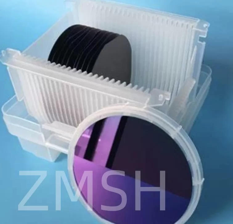
Physical photo of InP Laser Epitaxial Wafer:


EPl layer default structure of InP Laser Epitaxial Wafe:

Application of InP Laser Epitaxial Wafer:
Laser Diodes: Suitable for edge-emitting lasers and VCSELs.
Telecommunications: Vital for optical communication systems.
Sensing and Imaging: Used in optical sensors and imaging
applications.
Medical Devices: Employed in medical laser systems.
Application picture of InP Laser Epitaxial Wafer:

FAQ:
1.Q:What is an epitaxial wafer?
A:An epitaxial wafer (also called epi wafer, epi-wafer, or
epiwafer) is a wafer of semiconducting material made by epitaxial
growth (epitaxy) for use in photonics, microelectronics,
spintronics, or photovoltaics.
2.Q:What are the advantages of InP?
A:The Distinct Advantages InP Wafers Offer:High Electron Mobility:
InP exhibits electron mobility nearly ten times greater than
silicon, making it perfect for high-speed transistors and
amplifiers in telecommunications and radar systems.
Product recommend:
1.8inch
GaN-on-Si Epitaxy Si Substrate 110 111 110 for MOCVD Reactors Or RF
Energy Application

2.InP
wafer 2inch 3inch 4inch VGF P type N type Depant Zn S Fe Undoped
Prime Grade Testing Grade
Key word: InP Laser Epitaxial Wafe; InP


