Si wafer 4inch Polished CZ Dopant Arsenic(As) Boron(B)
Phosphorus(Ph) (100) Semiconductor
Describe of Si Wafer:
A Silicon wafer is a very thin round disk cut from high-purity
silicon. A round silicon ingot is sliced to thicknesses of
approximately 1mm. The surfaces of the resulting disk are polished
carefully, then it is cleaned, resulting in the completed wafer.
Silicon wafers are made from high-purity silicon and are the
material of semiconductor devices. These wafers can also be
fabricated with an SEMI notch or one or two SEMI flats. we specialize in producing high-quality polished silicon wafers
for semiconductor and electronics applications. Our 100mm polished
silicon wafers offer prime quality single crystal monocrystalline
material with tightly controlled electrical resistivity and
thickness variation specifications. This product consists of 100mm
diameter silicon wafers sliced from a single crystal ingot grown
using the Czochralski (CZ) method. They have been either
single-side polished or double-side polished to achieve exceptional
thickness uniformity, particle performance, surface microroughness,
and flatness specifications.
The Character of Si Wafer:
1. Premium Quality – All silicon wafers are brand new, virgin
silicon wafers – they have never been used or reused
2. Epi-Ready Surface – Our Prime grade silicon wafers have premium
epi-ready surfaces
3. Monocrystalline Material – All wafers are made from prime-grade
monocrystalline silicon material
4. Exceed Industry Standards – Our 100mm silicon wafers exceed SEMI
standard specifications and industry standards
5. Versatile Applications – Our 100mm silicon wafers are suitable
for a wide range of applications, including semiconductor
manufacturing, research and development, and educational purposes
6. Trusted by Industry Leaders – Our 100mm silicon wafers are
extensively used by leading semiconductor fabs, R&D centers,
universities, and pilot lines around the world
7. Quality Control and Inspection – Every wafer undergoes a
comprehensive quality inspection and testing
8. Secure Packaging – Wafers are packaged in dedicated ultra-clean
PP cassettes and double-bagged in antistatic bags under class 100
cleanroom conditions to protect the surface from particulate
contamination
9. Competitive Pricing – WaferPro offers competitive pricing with
quantity discounts available
10. Certificate of Conformance – A COC is included with each order
stating the exact specifications of the wafer.
The Form of Si Wafer:
| Product Name | 4-inch polished wafer |
| Material | Silicon |
| Diameter | 100±0.2mm |
| Thickness | 525±15um / as requested |
| Type/Dopant: | P/Boron or N/As |
| Resistivity | as request |
| Orientation | <100> |
| Grade | Prime/Test grade/ Test grade |
| Growth | CZ |
| Primary Flat Location | <110>±1 |
| Primary Flat Length | 32.5±2.5mm |
| Thickness Tolerance | 500±20μ m |
| TTV | <10μ m |
| TIR | <10um |
| Warp | <30μ m |
| Bow | <30μ m |
| Front Surface | Polishing |
| Back Surface | Grinding |
| Oxidation | Wet Oxidation |
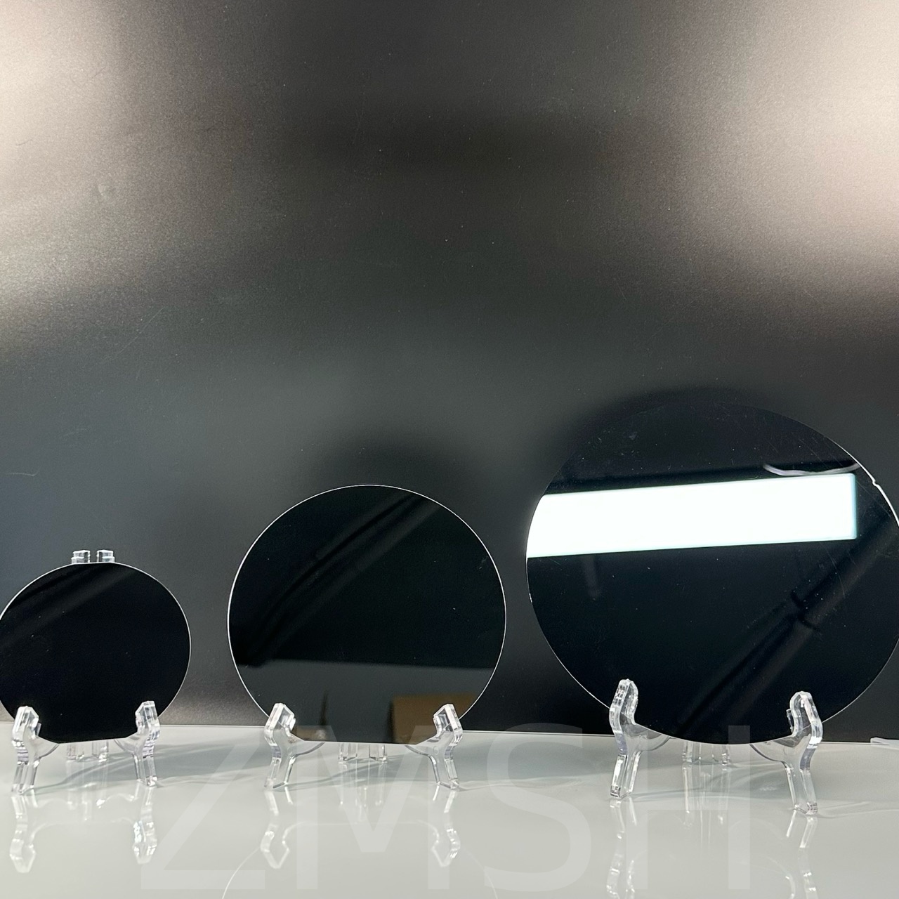
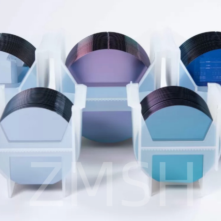
The Physical photo of Si Wafer:

The Application of Si Wafer:
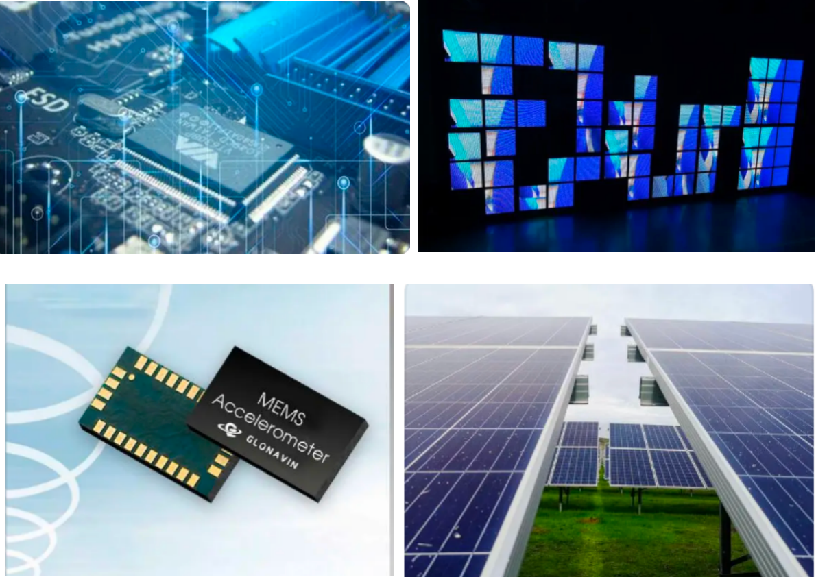
1. Microchip production and integrated circuit fabrication
2. MEMS and microelectromechanical systems
3. Semiconductor and sensor manufacturing
4. LED lighting and laser diode creation
5. Solar/photovoltaic cells and wafers
6. Optical equipment components
7. Insulated sandwich panels
8. R&D prototyping and testing
The Application Pictures of Si Wafer:
Customization:
We specialize in the processing and supply of various types of
high-quality silicon wafers. Our offerings include:
Single Crystal Silicon Wafers Growth Methods: CZ (Czochralski),
MCZ, and others.
Sizes: 2", 4", 5", 6", 8" as well as custom diameters and
non-standard shaped silicon wafers.
Surface Finishes: Single-side polished, double-side polished,
grinding, etc.
Conductivity Types: N-type, P-type, intrinsic semiconductors.
Specifications: Tailored to meet a wide range of applications.
Supply Capacity: Extensive inventory with various types available
in stock.
Processing Flexibility: Custom processing of various
specifications, tailored to meet customer requirements with short
lead times.
FAQ:
1. Q: What surface finishes can we supply?
A: We offer wafers with double-side polish (DSP), single-side
polish (SSP), or Etched/Etched surfaces. Please feel free to
contact us for your preferred specifications.
2. Q: What customizations are available?
A: Our capabilities include laser marking, wafer labeling, and
various edge modifications like cuts or notches to your exact
requirements.
3: Q: What sizes do you offer?
A: Besides our 4-inch (100mm) silicon wafers, we also supply sizes
of 2”, 3”, 150mm, 200mm, and 300mm diameter. Other custom sizes may
be available upon request.
Product Recommend:
1. Single
Crystal Si Wafer Electronic Device Substrate Photolithography Layer
2"3"4"6"8"

2. Silicon
Wafer CZ orientation111 Resistivity: 1-10 (ohm. cm) single side or
double side polish

 Boron(B) Phosphorus(Ph) (100) Semiconductor on sale")
 Boron(B) Phosphorus(Ph) (100) Semiconductor on sale")
 Boron(B) Phosphorus(Ph) (100) Semiconductor on sale")
 Boron(B) Phosphorus(Ph) (100) Semiconductor on sale")
 Boron(B) Phosphorus(Ph) (100) Semiconductor on sale")
 Boron(B) Phosphorus(Ph) (100) Semiconductor on sale")


