GaN on sapphire GaN Epitaxy Template on Sapphire 2inch 4inch 6inch
8inch
Abstract:
Gallium Nitride (GaN) on Sapphire epitaxy templates are
cutting-edge materials available in N-type, P-type, or
semi-insulating forms. These templates are designed for the
preparation of advanced semiconductor optoelectronic devices and
electronic devices. The core of these templates is a GaN epitaxial
layer grown on a sapphire substrate, resulting in a composite
structure that leverages the unique properties of both materials to
achieve superior performance.
Structure and Composition:
Gallium Nitride (GaN) Epitaxial Layer:
- Single Crystal Thin Film: The GaN layer is a single crystal thin film, which ensures high
purity and excellent crystallographic quality. This property is
essential for minimizing defects and dislocations, thereby
enhancing the performance of the devices fabricated on these
templates.
- Material Properties: GaN is known for its wide bandgap (3.4 eV), high electron
mobility, and high thermal conductivity. These properties make it
ideal for high-power and high-frequency applications, as well as
for devices that operate in harsh environments.
Sapphire Substrate:
- Mechanical Strength: Sapphire (Al2O3) is a robust material with exceptional mechanical
strength, which provides a stable and durable foundation for the
GaN layer.
- Thermal Stability: Sapphire has excellent thermal properties, including high thermal
conductivity and thermal stability, which help in dissipating heat
generated during device operation and maintaining device integrity
at high temperatures.
- Optical Transparency: The transparency of sapphire in the ultraviolet to infrared range
makes it suitable for optoelectronic applications, where it can
serve as a transparent substrate for emitting or detecting light.
Types of GaN on Sapphire Templates:
N-type GaN:
- Doping and Conductivity: N-type GaN is doped with elements such as silicon (Si) to
introduce free electrons, enhancing its electrical conductivity.
This type is widely used in devices like high-electron-mobility
transistors (HEMTs) and light-emitting diodes (LEDs), where high
electron concentration is crucial.
P-type GaN:
- Doping and Hole Conductivity: P-type GaN is doped with elements such as magnesium (Mg) to
introduce holes (positive charge carriers). P-type GaN is essential
for creating p-n junctions, which are the building blocks of many
semiconductor devices, including LEDs and laser diodes.
Semi-insulating GaN:
- Reduced Parasitic Capacitance: Semi-insulating GaN is used in applications where minimizing
parasitic capacitance and leakage currents is critical. This type
is ideal for high-frequency and high-power electronic devices,
ensuring stable performance and efficiency.
Manufacturing Processes:
Epitaxial Deposition:
- Metal-Organic Chemical Vapor Deposition (MOCVD): This technique is commonly used for growing high-quality GaN
layers on sapphire substrates. MOCVD allows precise control over
the film thickness, composition, and doping levels, resulting in
uniform and defect-free layers.
- Molecular Beam Epitaxy (MBE): Another method for growing GaN layers, MBE offers excellent
control at the atomic level, which is beneficial for research and
development of advanced device structures.
Diffusion:
- Controlled Doping: The diffusion process is used to introduce dopants into specific
regions of the GaN layer, modifying its electrical properties to
suit various device requirements.
Ion Implantation:
- Precise Doping and Damage Repair: Ion implantation is a technique for introducing dopants with high
precision. Post-implantation annealing is often used to repair any
damage caused by the implantation process and activate the dopants.
Special Features:
- Non-PS (SSP) Templates: These templates are designed to be used alongside PS wafers for
planar runs, which can help achieve clearer reflectance
measurements. This feature is particularly useful in quality
control and optimization of optoelectronic devices.
- Low Lattice Mismatch: The lattice mismatch between GaN and sapphire is relatively low,
reducing the number of defects and dislocations in the epitaxial
layer. This results in better material quality and improved
performance of the final devices.
Applications:
- Optoelectronic Devices: GaN on Sapphire templates are widely used in LEDs, laser diodes,
and photodetectors. The high efficiency and brightness of GaN-based
LEDs make them ideal for general lighting, automotive lighting, and
display technologies.
- Electronic Devices: The high electron mobility and thermal stability of GaN make it
suitable for high-electron-mobility transistors (HEMTs), power
amplifiers, and other high-frequency and high-power electronic
components.
- High-Power and High-Frequency Applications: GaN on Sapphire is essential for applications requiring high
power and high-frequency operation, such as RF amplifiers,
satellite communication, and radar systems.


For more detailed specifications of GaN on Sapphire, including
electrical, optical, and mechanical properties, please refer to the
following sections. This detailed overview highlights the
versatility and advanced capabilities of GaN on Sapphire templates,
making them an optimal choice for a wide range of semiconductor
applications.
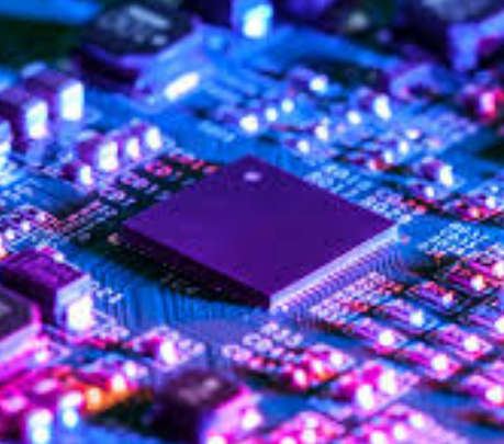
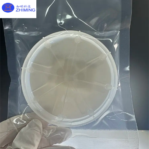
Photos:

Properties:
Electrical Properties:
Wide Bandgap:
- GaN: Approximately 3.4 eV
- Allows for high-voltage operation and better performance in
high-power applications.
High Breakdown Voltage:
- GaN can withstand high voltages without breaking down, making it
ideal for power devices.
High Electron Mobility:
- Facilitates fast electron transport, leading to high-speed
electronic devices.
Thermal Properties:
High Thermal Conductivity:
- GaN: Approximately 130 W/m·K
- Sapphire: Approximately 42 W/m·K
- Efficient heat dissipation, crucial for high-power devices.
Thermal Stability:
- Both GaN and sapphire maintain their properties at high
temperatures, making them suitable for harsh environments.
Optical Properties:
Transparency:
- Sapphire is transparent in the UV to IR range.
- GaN is typically used for blue to UV light emission, important for
LEDs and laser diodes.
Refractive Index:
- GaN: 2.4 at 632.8 nm
- Sapphire: 1.76 at 632.8 nm
- Important for designing optoelectronic devices.
Mechanical Properties:
Hardness:
- Sapphire: 9 on the Mohs scale
- Provides a durable substrate that resists scratching and damage.
Lattice Structure:
- GaN has a wurtzite crystal structure.
- The lattice mismatch between GaN and sapphire is relatively low
(~16%), which helps in reducing defects during epitaxial growth.
Chemical Properties:
- Chemical Stability:
- Both GaN and sapphire are chemically stable and resistant to most
acids and bases, which is important for device reliability and
longevity.
These properties highlight why GaN on Sapphire is extensively used
in modern electronic and optoelectronic devices, offering a
combination of high efficiency, durability, and performance under
demanding conditions.


