Silicon-on-Insulator SOI wafer 6", 2.5 "m (P-doped ) + 1.0 SiO2 + 625um Si (P-type /Boron doped )
Silicon-on-Insulator (SOI) Wafer Abstract
This Silicon-on-Insulator (SOI) wafer is a specialized semiconductor substrate designed for advanced electronic and microelectromechanical systems (MEMS) applications. The wafer is characterized by a multi-layer structure that enhances device performance, reduces parasitic capacitance, and improves thermal isolation, making it an ideal choice for a wide range of high-performance and high-precision applications.
Silicon-on-Insulator (SOI) Wafer Product Properties
Wafer Specifications:
- Wafer Diameter: 6 inches (150 mm)
- The 6-inch diameter provides a large surface area for device fabrication, improving manufacturing efficiency and reducing production costs.
Device Layer:
- Thickness: 2.5 micrometers
- The thin device layer allows for precise control of electronic properties, essential for high-speed and high-performance applications.
- Doping: P-type (Phosphorus-doped)
- Phosphorus doping enhances the electrical conductivity of the device layer, making it suitable for various p-type semiconductor devices.
Buried Oxide (BOX) Layer:
- Thickness: 1.0 micrometer
- The 1.0 μm thick SiO2 layer provides excellent electrical isolation between the device layer and the handle wafer, reducing parasitic capacitance and improving signal integrity.
Handle Wafer:
- Thickness: 625 micrometers
- The thick handle wafer ensures mechanical stability during fabrication and operation, preventing warping or breakage.
- Type: P-type (Boron-doped)
- Boron doping improves the mechanical strength and thermal conductivity of the handle wafer, aiding in heat dissipation and enhancing overall device reliability.
| Device Layer |
| Diameter: | | 6" |
| Type/Dopant: | | N type/P-doped |
| Orientation: | | <1-0-0>+/-.5 degree |
| Thickness: | | 2.5±0.5µm |
| Resistivity: | | 1-4 ohm-cm |
| Finish: | | Front Side Polished |
| Buried Thermal Oxide: |
| Thickness: | | 1.0um +/- 0.1 um |
| Handle Wafers: |
| Type/Dopant | | P Type, B doped |
| Orientation | | <1-0-0>+/-.5 degree |
| Resistivity: | | 10-20 ohm-cm |
| Thickness: | | 625 +/- 15 um |
| Finish: | | As-received (not polished) |
Key Product Properties:
-
High-Quality Device Layer:
- Carrier Mobility: High carrier mobility in the phosphorus-doped layer ensures fast electronic response and high-speed operation.
- Low Defect Density: The high-quality fabrication process ensures minimal defects, leading to better performance and higher yields.
-
Efficient Electrical Isolation:
- Low Parasitic Capacitance: The BOX layer effectively isolates the device layer from the substrate, reducing parasitic capacitance and crosstalk, crucial for high-frequency and low-power applications.
- Signal Integrity: Enhanced electrical isolation helps maintain signal integrity, which is essential for high-precision analog and digital circuits.
-
Thermal Management:
- Thermal Conductivity: The boron-doped handle wafer provides good thermal conductivity, aiding in the dissipation of heat generated during device operation, thus preventing overheating and ensuring stable performance.
- Heat Resistance: The wafer's structure and materials ensure it can withstand high temperatures during processing and operation.
-
Mechanical Stability:
- Robustness: The thick handle wafer provides mechanical support, ensuring the wafer remains stable during the fabrication process and under operational stresses.
- Durability: The mechanical stability of the handle wafer helps prevent damage, reducing the risk of wafer breakage and improving overall device longevity.
-
Versatility in Applications:
- High-Performance Computing: Suitable for processors and other high-speed digital logic circuits, thanks to its high carrier mobility and low parasitic capacitance.
- 5G Communication: Ideal for RF components and high-frequency signal processing, benefiting from the excellent electrical isolation and thermal management properties.
- MEMS Devices: Perfect for MEMS fabrication, offering the mechanical stability and precision needed for microfabricated structures.
- Analog and Mixed-Signal Circuits: The low noise and reduced crosstalk make it suitable for high-precision analog circuits.
- Power Electronics: The robust thermal and mechanical properties make it suitable for power management applications requiring high efficiency and reliability.
Conclusion
This Silicon-on-Insulator (SOI) wafer offers a unique combination of high-quality materials and advanced fabrication techniques, resulting in a substrate that excels in electrical performance, thermal management, and mechanical stability. These properties make it an ideal choice for a wide range of high-performance electronic and MEMS applications, supporting the development of next-generation semiconductor devices.
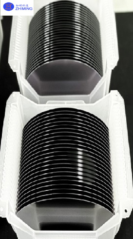
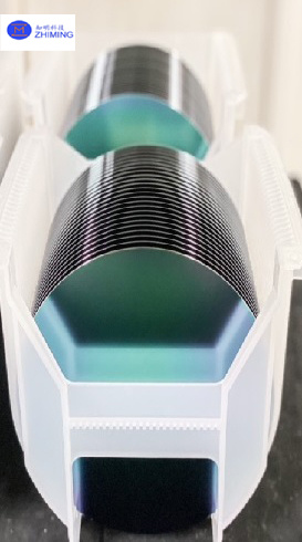
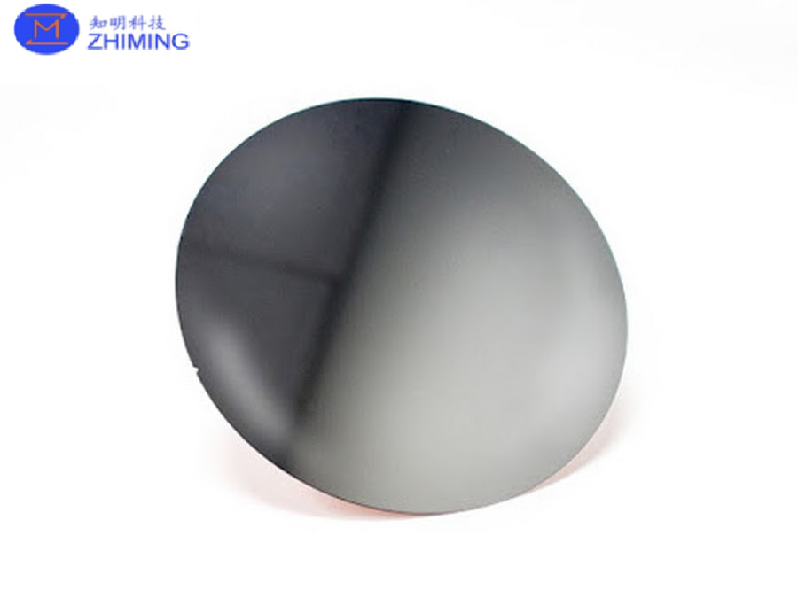
Silicon-on-Insulator (SOI) Wafer Product photos


Q&A
What Are SOI Wafers (Silicon-On-Insulator Wafers)?
Silicon-On-Insulator (SOI) wafers are a type of semiconductor substrate that consist of multiple layers, including a thin silicon device layer, an insulating oxide layer, and a supporting silicon handle wafer. This structure enhances the performance of semiconductor devices by providing better electrical isolation, reducing parasitic capacitance, and improving thermal management.
SHANGHAI FAMOUS TRADE CO.,LTD
SHANGHAI FAMOUS TRADE CO.,LTD. locates in the city of Shanghai,
Which is the best city of China, and our factory is founded in Wuxi
city in 2014.
We specialize in processing a varity of materials into wafers,
substrates and custiomized optical glass parts.components widely
used in electronics, optics, optoelectronics and many other fields.
We also have been working closely with many domestic and oversea
universities, research institutions and companies, provide
customized products and services for their R&D projects.
It's our vision to maintaining a good relationship of cooperation
with our all customers by our good reputatiaons.

 + 1.0 SiO2 + 625um Si (P-type /Boron Doped ) on sale")
 + 1.0 SiO2 + 625um Si (P-type /Boron Doped ) on sale")
 + 1.0 SiO2 + 625um Si (P-type /Boron Doped ) on sale")
 + 1.0 SiO2 + 625um Si (P-type /Boron Doped ) on sale")
 + 1.0 SiO2 + 625um Si (P-type /Boron Doped ) on sale")
 + 1.0 SiO2 + 625um Si (P-type /Boron Doped ) on sale")


