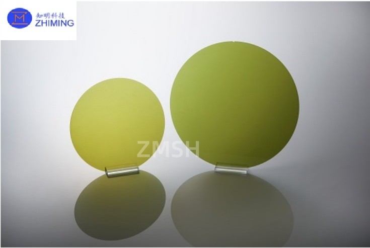
SiC seed crystals, specifically those with diameters of 153, 155,
205, 203, and 208 mm
Abstract of the SiC seed crystals
SiC seed crystals are small crystals with the same crystal
orientation as the desired crystal, serving as seeds for single
crystal growth. Different orientations of seed crystals yield
single crystals with varying orientations. Based on their
applications, seed crystals can be categorized into CZ
(Czochralski) pulled single crystal seeds, zone-melted seeds,
sapphire seeds, and SiC seeds.
SiC materials possess advantages such as a wide bandgap, high
thermal conductivity, high critical breakdown field strength, and
high saturated electron drift velocity, making them highly
promising in semiconductor manufacturing.
SiC seed crystals play a crucial role in the semiconductor
industry, and their preparation processes are vital for crystal
quality and growth efficiency. Choosing and preparing suitable SiC
seed crystals is foundational for SiC crystal growth. Different
growth methods and control strategies directly impact the quality
and performance of the crystals. Researching the thermodynamic
properties and growth mechanisms of SiC seed crystals helps
optimize production processes, enhancing both crystal quality and
yield.

The Attribute Table of the SiC seed crystals
| Property | Value / Description | Unit / Notes |
| Crystal Structure | 4H, 6H, 3C (most common: 4H for power devices) | Polytypes vary in stacking sequence |
| Lattice Parameters | a=3.073Å, c=10.053Å (4H-SiC) | Hexagonal system |
| Density | 3.21 | g/cm³ |
| Melting Point | 3100 (sublimes) | °C |
| Thermal Conductivity | 490 (∥c), 390 (⊥c) (4H-SiC) | W/(m·K) |
| Thermal Expansion | 4.2×10⁻⁶ (∥c), 4.68×10⁻⁶ (⊥c) | K⁻¹ |
| Band Gap | 3.26 (4H), 3.02 (6H), 2.36 (3C) | eV /300K |
| Hardness (Mohs) | 9.2-9.6 | Second only to diamond |
| Refractive Index | 2.65 633nm (4H-SiC) | |
| Dielectric Constant | 9.66 (∥c), 10.03 (⊥c) (4H-SiC) | 1MHz |
| Breakdown Field | ~3×10⁶ | V/cm |
| Electron Mobility | 900-1000 (4H) | cm²/(V·s) |
| Hole Mobility | 100-120 (4H) | cm²/(V·s) |
| Dislocation Density | <10³ (best commercial seeds) | cm⁻² |
| Micropipe Density | <0.1 (state-of-the-art) | cm⁻² |
| Off-cut Angle | Typically 4° or 8° toward <11-20> | For step-controlled epitaxy |
| Diameter | 153mm , 155mm , 203mm | Commercial availability |
| Surface Roughness | <0.2nm (epi-ready) | Ra (atomic level polishing) |
| Orientation | (0001) Si-face or C-face | Affects epitaxial growth |
| Resistivity | 10²-10⁵ (semi-insulating) | Ω·cm |
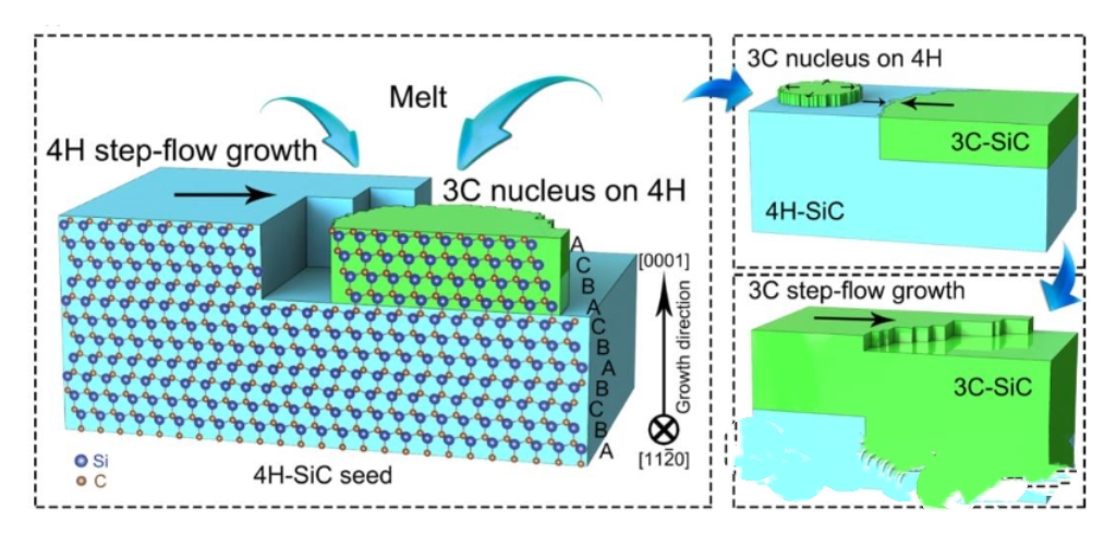
Physical vapor transport (PVT) methods
Typically, SiC single crystals are generated using physical vapor
transport (PVT) methods. The process involves placing SiC powder at
the bottom of a graphite crucible, with the SiC seed crystal
positioned at the top. The graphite crucible is heated to the
sublimation temperature of SiC, causing the SiC powder to decompose
into vapor species such as Si vapor, Si2C, and SiC2. Under the
influence of an axial temperature gradient, these gases rise to the
top of the crucible, where they condense on the surface of the SiC
seed crystal, forming SiC single crystals.
Currently, the diameter of the seed crystal used for SiC single
crystal growth must match that of the target crystal. During
growth, the seed crystal is fixed to a seed holder at the top of
the crucible using adhesive. However, issues such as surface
processing accuracy of the seed holder and uniformity of the
adhesive application can lead to pore formation at the adhesive
interface, resulting in hexagonal void defects.
To address the issue of adhesive layer density, various solutions
have been proposed by companies and research institutions,
including improving the flatness of graphite plates, increasing the
uniformity of adhesive film thickness, and incorporating flexible
buffer layers. Despite these efforts, problems with adhesive layer
density persist, and there is a risk of seed crystal detachment. A
solution involving bonding the wafer to graphite paper that
overlaps the top of the crucible has been implemented, effectively
resolving the adhesive layer density issue and preventing seed
crystal detachment.

Q&A
Q:What factors affect the quality of SiC seed crystals?
A:1. Crystalline Perfection
2. Polytype Control
3. Surface Quality
4. Thermal/Mechanical Properties
5. Chemical Composition
6. Geometric Parameters
7. Process-Induced Factors
8. Metrology Limitations
Other related products
2/4/6/8
inch SiC wafer