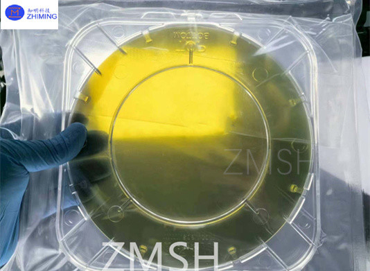
SiC seed crystals diameters of 153, 155, 205, 203, and 208 mm PVT
Abstract of the SiC Seed Crystals
Silicon carbide (SiC) has emerged as a vital material in the
semiconductor industry due to its unique properties, such as a wide
bandgap, high thermal conductivity, and exceptional mechanical
strength. SiC seed crystals play a crucial role in the growth of
high-quality SiC single crystals, which are essential for various
applications, including high-power and high-frequency devices.
SiC seed crystals are small crystalline structures that serve as
the starting point for the growth of larger SiC single crystals.
They possess the same crystal orientation as the desired final
product, allowing for the continuation of the crystal lattice
structure during growth. The seed crystal acts as a template,
guiding the arrangement of atoms in the growing crystal.
The Attribute Table of the SiC Seed Crystal
| Property | Value / Description | Unit / Notes |
| Crystal Structure | 4H, 6H, 3C (most common: 4H for power devices) | Polytypes vary in stacking sequence |
| Lattice Parameters | a=3.073Å, c=10.053Å (4H-SiC) | Hexagonal system |
| Density | 3.21 | g/cm³ |
| Melting Point | 3100 (sublimes) | °C |
| Thermal Conductivity | 490 (∥c), 390 (⊥c) (4H-SiC) | W/(m·K) |
| Thermal Expansion | 4.2×10⁻⁶ (∥c), 4.68×10⁻⁶ (⊥c) | K⁻¹ |
| Band Gap | 3.26 (4H), 3.02 (6H), 2.36 (3C) | eV /300K |
| Hardness (Mohs) | 9.2-9.6 | Second only to diamond |
| Refractive Index | 2.65 @ 633nm (4H-SiC) | |
| Dielectric Constant | 9.66 (∥c), 10.03 (⊥c) (4H-SiC) | 1MHz |
| Breakdown Field | ~3×10⁶ | V/cm |
| Electron Mobility | 900-1000 (4H) | cm²/(V·s) |
| Hole Mobility | 100-120 (4H) | cm²/(V·s) |
| Dislocation Density | <10³ (best commercial seeds) | cm⁻² |
| Micropipe Density | <0.1 (state-of-the-art) | cm⁻² |
| Off-cut Angle | Typically 4° or 8° toward <11-20> | For step-controlled epitaxy |
| Diameter | 100mm (4"), 150mm (6"), 200mm (8") | Commercial availability |
| Surface Roughness | <0.2nm (epi-ready) | Ra (atomic level polishing) |
| Orientation | (0001) Si-face or C-face | Affects epitaxial growth |
| Resistivity | 10²-10⁵ (semi-insulating) | Ω·cm |
Diameters of SiC Seed Crystals

The typical diameters for SiC seed crystals range from 153 mm to
208 mm, including specific sizes such as 153 mm, 155 mm, 203 mm,
205 mm, and 208 mm. These dimensions are selected based on the
intended application and the desired size of the resulting single
crystal.
1. 153 mm and 155 mm Seed Crystals
These smaller diameters are often used for initial experimental
setups or for applications that require smaller wafers. They allow
researchers to explore various growth conditions and parameters
without the need for larger, more costly equipment.
2. 203 mm and 205 mm Seed Crystals
Mid-range diameters like these are commonly used for industrial
applications. They provide a balance between material usage and the
size of the final single crystals. These sizes are often employed
in the production of power electronics and high-frequency devices.
3. 208 mm Seed Crystals
The largest seed crystals available, such as those with a diameter
of 208 mm, are typically utilized for high-volume production. They
enable the growth of larger single crystals, which can be sliced
into multiple wafers for manufacturing. This size is particularly
advantageous in the automotive and aerospace industries, where
high-performance components are essential.
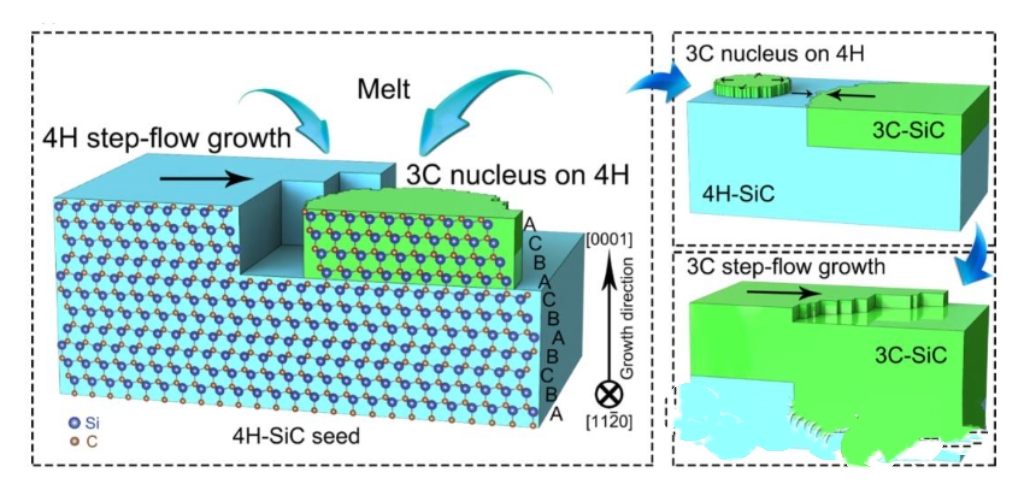
Growth Methods for SiC Seed Crystals
The growth of SiC single crystals usually involves several methods,
with the physical vapor transport (PVT) method being the most
prevalent. This process is characterized by the following steps:
Preparation of the Graphite Crucible: SiC powder is placed at the
bottom of a graphite crucible. The crucible is then heated to the
sublimation temperature of SiC.
Placement of the Seed Crystal: The SiC seed crystal is positioned
at the top of the crucible. As the temperature gradients are
established, the SiC powder sublimates into a vapor.
Condensation: The vapor rises to the top of the crucible, where it
condenses on the surface of the SiC seed crystal, facilitating the
growth of the single crystal.
Thermodynamic Properties
The thermodynamic behaviors of SiC during the growth process are
critical. The temperature gradient and pressure conditions must be
carefully controlled to ensure optimal growth rates and crystal
quality. Understanding these properties aids in refining growth
techniques and improving yield.
Challenges in SiC Seed Crystal Production
While the growth of SiC seed crystals is well-established, several
challenges persist:
1. Adhesive Layer Density
When attaching seed crystals to the growth holders, issues such as
the uniformity of the adhesive layer can lead to defects. Poor
adhesion can result in voids or detachment during the growth
process.
2. Surface Quality
The surface quality of the seed crystal is crucial for successful
growth. Any imperfections can propagate through the crystal
lattice, leading to defects in the final product.
3. Cost and Scalability
Producing larger SiC seed crystals is often more expensive and
requires advanced manufacturing techniques. Balancing cost with
quality and scalability remains a challenge for the industry.
Q&A
Q:What's the most common orientations used in SiC growth?
A: Different orientations of SiC seed crystals yield single crystals
with varying characteristics. The most common orientations used in
SiC growth are 4H-SiC and 6H-SiC, each with distinct electrical and
thermal properties. The choice of orientation affects the
performance of the final device, making the selection of the
appropriate seed crystal crucial.


