Product Overview
TGV Sapphire is a transparent conductive glass material based on
sapphire (Al₂O₃) substrates, coated with transparent conductive
oxide (TCO) films (e.g., ITO, AZO) via magnetron sputtering. TGV
Sapphire combines sapphire’s ultra-high hardness, high-temperature
resistance, and TCO films’ conductivity and transparency, making it
ideal for high-performance electronic devices in extreme
environments.
Principle
Using laser drilling or dry etching, vertical vias with high aspect ratios are created in the sapphire substrate. These vias are metallized to enable vertical electrical signal transmission, while maintaining the sapphire’s optical clarity and mechanical integrity.
Sapphire Substrate: Sapphire (Al₂O₃) is one of the hardest oxide materials in nature,
offering exceptional chemical stability, high thermal conductivity
(~40 W/m·K), and a wide optical bandgap (~9.9 eV), enabling
resistance to high temperatures and harsh chemical environments.
Transparent Conductive Layer: A nano-scale TCO film (e.g., ITO) is deposited on the sapphire
surface via physical vapor deposition (PVD), balancing high
transmittance (>90%) and low sheet resistance (≤10 Ω/sq).
Technical Challenges
Extreme Hardness
Sapphire has a Mohs hardness of 9 (second only to diamond), making
traditional mechanical drilling tools (e.g., tungsten carbide
drills) prone to rapid wear or even ineffective.
Brittle Fracture Risk
Sapphire’s single-crystal structure makes it susceptible to
micro-cracks, edge chipping, or delamination during machining,
compromising hole-wall quality and device reliability.
Micro-Hole Requirements
For LED chips or MEMS sensors, holes with diameters <100 μm are
often needed, requiring precision within ±1 μm.
Thermal Damage Control
High-temperature processes (e.g., laser drilling) may cause
localized melting or thermal stress cracks.
Specification
| Item | Typical Values (Customizable) |
|---|
| Material | Single-crystal Sapphire (C-plane, A-plane optional) |
| Thickness | 100 μm – 1000 μm |
| Via Diameter | ≥ 20 μm |
| Aspect Ratio | ≥ 10:1 |
| Via Density | > 1,000,000 vias/cm² (optional) |
| Metallization | Ti/Cu, Ni/Au, Pt, etc. |
| Surface Roughness | Ra < 1 nm (polishing available) |
| Package Compatibility | Fan-out, Flip-chip, MEMS packaging, etc. |
Applications
Consumer Electronics: Scratch-resistant AR/VR displays, flexible
OLED backplanes.

Optoelectronics: Laser window components, UV sensors,
high-power LED substrates.

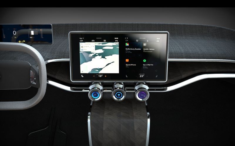
Automotive: Automotive displays, LiDAR optical components.
Aerospace: Radiation-resistant satellite parts and spacecraft
windows.

Q&A
Q1: What’s the difference between TGV Sapphire and ordinary
conductive glass?
A1: TGV Sapphire is 10x harder than regular glass, withstands
temperatures up to 600℃, and operates in harsh chemical
environments.
Q2: Can TGV Sapphire be customized (e.g., shape cutting,
thickness adjustment)?
A2: Yes, customizable dimensions, thickness (0.5mm~5mm), and
conductive layer patterns are available.
Q3: Does extreme temperature affect TGV Sapphire conductivity?
A3: Sapphire’s CTE matches silicon chips, ensuring stable
conductivity under high temperatures.
Related products


