Product Overview
TGV (Through Glass Via) technology, also known as glass
through-hole technology, is a vertical electrical interconnection
technique that penetrates glass substrates. It enables vertical
electrical connections on glass substrates, achieving high-density
interconnections between chips, as well as between chips and
substrates. While TSV (Through Silicon Via) technology is used for
interposers in silicon-based substrates, TGV serves the same
purpose in glass-based substrates.
Glass substrates represent the next generation of chip base
materials, with glass as their core component. The key enabling
technology for glass substrate packaging is TGV. The glass
substrate industry chain encompasses production, raw materials,
equipment, technology, packaging, testing, and applications, with
upstream segments focusing on production, materials, and equipment.
Advantages
- Superior High-Frequency Electrical Performance
- Ease of Obtaining Large-Scale Ultra-Thin Glass Substrates
- Cost Efficiency
- Simplified Process Flow
- Strong Mechanical Stability
- Broad Application Potential
Technical Principles


(a) Prepare glass wafers
(b) Form TGVs (Through Glass Vias)
(c) Deposit PVD barrier layer and seed layer, perform dual-side
electroplating for copper deposition
(d) Annealing and CMP (Chemical Mechanical Polishing) to remove
surface copper layer
(e) PVD coating and photolithography
(f) Fabricate RDL (Redistribution Layer)
(g) Strip photoresist and perform Cu/Ti etching
(h) Form passivation layer (dielectric layer)
Detailed steps:
The TGV (Through Glass Via) fabrication process begins with
incoming material inspection, followed by via formation through
methods including sandblasting, ultrasonic drilling, wet etching,
deep reactive ion etching (DRIE), photosensitive etching, laser
etching, laser-induced deep etching, and focused discharge
drilling, subsequently undergoing via inspection and cleaning.
Through Glass Vias (TGVs) are fabricated using plasma etching
technology.

After the hole is formed, it is necessary to inspect the hole, such
as through-hole rate, foreign matter, panel defects, etc.
Via Integrity – Detect leaks and non-conductive vias. Aperture size
specifications: 10/30/50/70/100 µm; outer diameter must exceed
inner diameter by ≥60%. Defect criteria: area; circularity (≥95%
control); diameter tolerance (±5 µm).
Foreign Material in Vias – Check continuity and detect residues
(glass debris, carbon fibers, adhesives, dust).
Panel Defects – Cracks, etching defects (pits), contaminants,
scratches.

Again, electroplating from bottom to top achieves seamless filling
of TGV;

Finally, temporary bonding, back grinding, chemical mechanical
polishing (CMP) to expose copper, debonding, and forming a
through-glass via (TGV) process technology metal-filled transfer
board. During the process, semiconductor processes such as cleaning
and testing are also required.
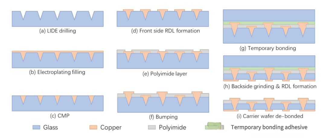
(a) LIDE drilling
(b) Electroplating filling
(c) CMP
(d) Front side RDL formation
(e) Polyimide layer
(f) Bumping
(g) Temporary bonding
(h) Backside grinding & RDL formation
(i) Carrier wafer de-bonded
Applications
High-frequency communications (5G/6G chip packaging)
High-performance computing and AI chips
Autonomous LiDAR modules, automotive radar, EV control units.
Implantable devices (e.g., neural probes), high-throughput
biochips.


Q&A
Q1:What is TGV glass?
A1:TGV glass: A glass substrate with vertical conductive vias for
high-density chip interconnection, suitable for high-frequency and
3D packaging.
Q2:What is the difference between glass substrate and silicon
substrate?
A2:
- Materials: Glass is an insulator (low dielectric loss), silicon is
a semiconductor.
- High-frequency performance: Glass signal loss is 10-100 times lower
than silicon.
- Cost: Glass substrate costs about 1/8 of silicon.
- TGV (Through Glass Via): A metallized vertical channel formed on a
glass substrate, without the need for an additional insulating
layer, and a simpler process than through silicon via (TSV).
Q3: Why Choose Glass Core Substrates?
A3:
- High-Frequency Superiority:Low Dk/Df minimizes signal distortion in
5G/6G mmWave bands (24-300 GHz).
- Cost Efficiency:Large-area panel processing (e.g., Gen 8.5 glass
panels) reduces costs by 70% vs. silicon wafers.
- Thermal & Mechanical Stability:Near-zero warpage even at ultra-thin
(<100 µm) thicknesses.CTE tunability reduces thermal stress in
multi-material systems.
- Optical Transparency:Enables hybrid electrical/optical integration
(e.g., LiDAR, AR displays).
- Scalability:Supports panel-level packaging (PLP) for mass
production of advanced 3D ICs.
Related products