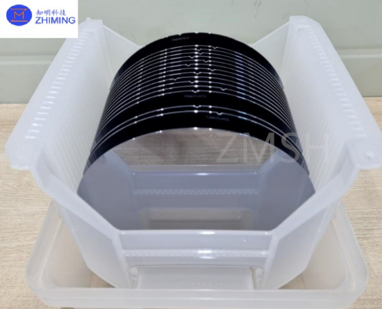
SOI wafer P Type N Type 6 inch 8 inch 12 inch Surface polish
SSP/DSP
Abstract of SOI wafer
Silicon on Insulator (SOI) is an advanced semiconductor technology
where a thin insulating layer, typically silicon dioxide (SiO₂), is
inserted between the silicon substrate and the active silicon
layer. This structure significantly reduces parasitic capacitance,
improves switching speed, lowers power consumption, and enhances
radiation resistance compared to traditional bulk silicon
technology.
SOI stands for silicon-on-insulator, or Silicon On a substrate,
which introduces a layer of buried oxide between the top layer of
silicon and the underlying substrate.
SOI specification
| Thermal Conductivity | Relatively high thermal conductivity |
| Active Layer Thickness | Typically ranges from a few to several tens of nanometers (nm) |
| Wafer Diameter | 6 inches, 8 inches, 12 inches |
| Process Advantages | Higher device performance and lower power consumption |
| Performance Advantages | Excellent electrical properties, reduced
device size, minimized crosstalk between electronic components |
| Resistivity | Typically ranges from several hundred to thousands of ohm-cm |
| Power Consumption Characteristics | Low power consumption |
| Impurity Concentration | Low impurity concentration |
| Silicon Support on Insulator Wafer | SOI Silicon Wafer 4-inch, CMOS Three-Layer Structure |
Structure of SOI
SOI wafers typically consist of three main layers:
1.Top Silicon Layer (Device Layer): The thin silicon layer where semiconductor devices are
fabricated. The thickness varies from a few nanometers to tens of
micrometers depending on the application.
2.Buried Oxide (BOX) Layer: A thin layer of silicon dioxide (SiO₂) that provides electrical
insulation. It ranges in thickness from tens of nanometers to a few
micrometers.
3.Handle Wafer (Substrate): A mechanical support layer, usually made of bulk silicon or other
high-performance materials.
The thickness of both the top silicon and buried oxide layers can
be customized to optimize performance for specific applications.
SOI Manufacturing Processes
SOI wafers are produced using three primary methods:
1.SIMOX (Separation by IMplanted OXygen)
Involves implanting oxygen ions into a silicon wafer and oxidizing
them at high temperatures to form a buried oxide layer.
Produces high-quality SOI wafers but is relatively expensive.
2.Smart Cut™ (Developed by Soitec, France)
Uses hydrogen ion implantation and wafer bonding to create SOI
structures.
The most widely used method in commercial SOI production.

3.Wafer Bonding & Etch-Back
Involves bonding two silicon wafers and selectively etching one to
the desired thickness.
Used for thick SOI and specialized applications.
Applications of SOI
Due to its unique performance benefits, SOI technology is widely
adopted in various industries:
1.High-Performance Computing (HPC)
Companies like IBM and AMD use SOI in high-end server CPUs to boost
processing speeds and reduce power consumption.
SOI is widely used in supercomputers and AI processors.

2.Mobile & Low-Power Devices
FD-SOI technology is used in smartphones, wearables, and IoT
devices to balance performance and power efficiency.
Chipmakers like STMicroelectronics and GlobalFoundries produce
FD-SOI chips for low-power applications.

3.RF & Wireless Communication (RF SOI)
RF SOI is widely adopted in 5G, Wi-Fi 6E, and millimeter-wave
communication.
Used in RF switches, low-noise amplifiers (LNA), and RF front-end
modules (RF FEM).

4.Automotive Electronics
Power SOI is extensively used in electric vehicles (EVs) and
advanced driver assistance systems (ADAS).
It enables high-temperature and high-voltage operation, ensuring
reliability in harsh conditions.

5.Silicon Photonics & Optical Applications
SOI substrates are used in silicon photonics chips for high-speed
optical communication.
Applications include data centers, high-speed optical
interconnects, and LiDAR (Light Detection and Ranging).
Advantages of SOI wafer
1.Reduced parasitic capacitance and increased operating speed – Compared to bulk silicon materials, SOI devices achieve a speed
improvement of 20-35%.
2.Lower power consumption – Due to reduced parasitic capacitance and minimized leakage
current, SOI devices can lower power consumption by 35-70%.
3.Elimination of latch-up effects – SOI technology prevents latch-up, improving device reliability.
4.Suppression of substrate noise and reduced soft errors – SOI effectively mitigates pulse current interference from the
substrate, decreasing the occurrence of soft errors.
5.Compatibility with existing silicon processes – SOI technology integrates well with conventional silicon
fabrication, reducing processing steps by 13-20%.
Tag:# SOI wafer # P Type # N Type # 6 inch # 8 inch #12 inch # Surface
polish SSP/DSP


