| Sign In | Join Free | My himfr.com |
|

SHANGHAI FAMOUS TRADE CO.,LTD
SHANGHAI FAMOUS TRADE CO.,LTD
Verified Supplier
7 Years
- Home
-
Products
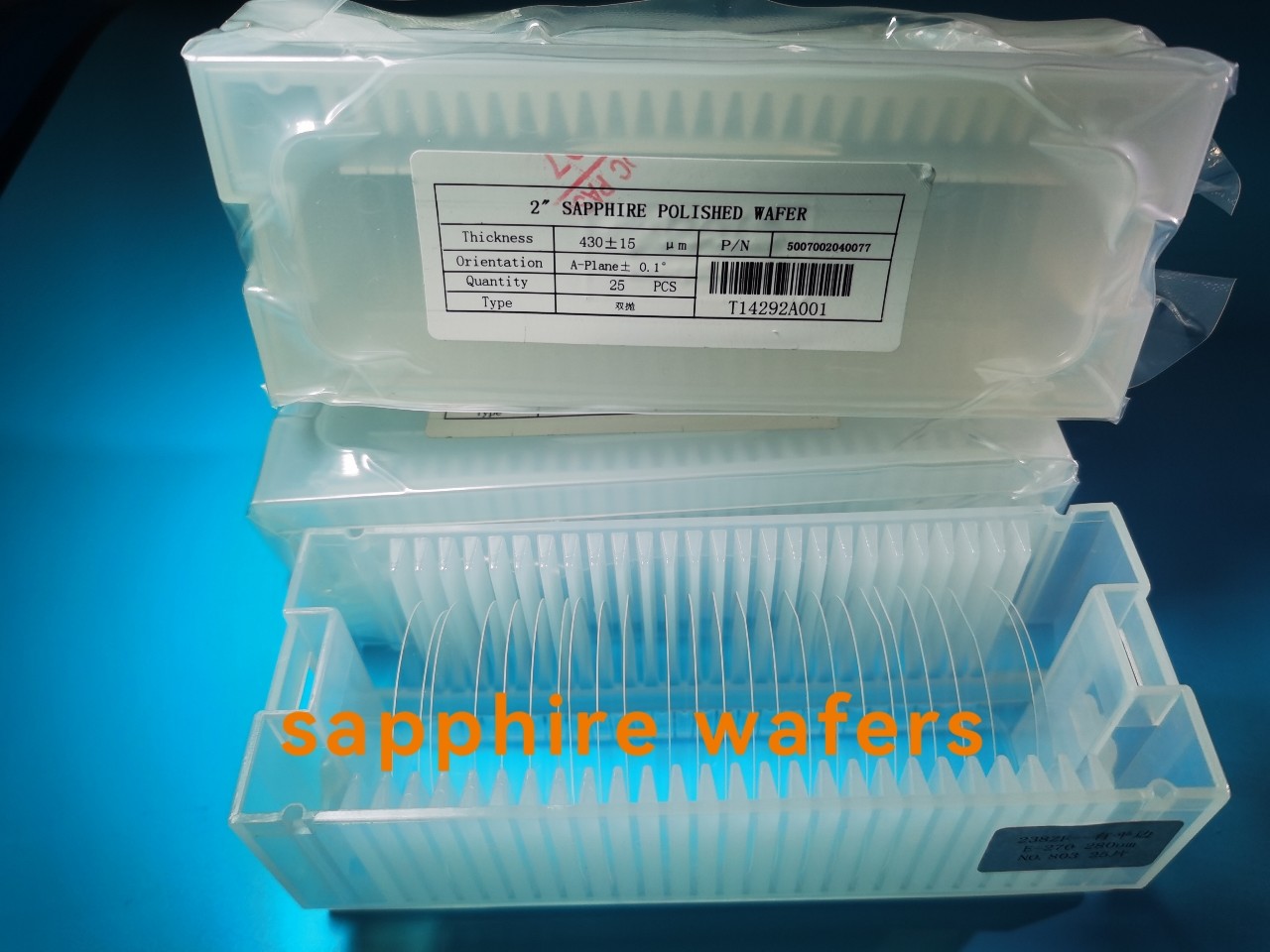
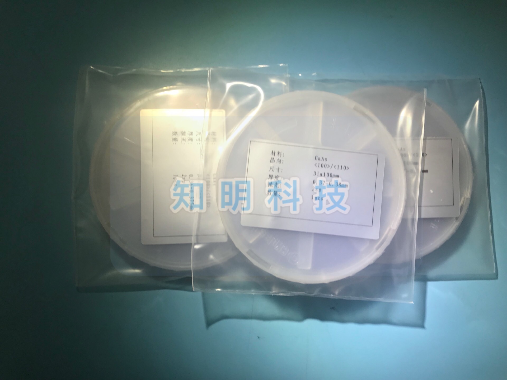
- Sapphire Substrate(89)
- Synthetic Gem Stone(75)
- Sapphire Optical Windows(86)
- Silicon Carbide Wafer(104)
- Sapphire Tube(62)
- Gallium Nitride Wafer(25)
- Semiconductor Substrate(103)
- Scientific Lab Equipment(50)
- Sapphire Crystal Watch Case(19)
- Wafer Carrier Box(14)
- Superconducting Thin Monocrystalline Substrate(13)
- Ceramic Parts(7)
- About Us
- Quality Control
- Contact Us
- Get Quotations