6 Inch 153mm 156mm 159mm Thickness 350um 0.5mmt Sapphire Carrier
Substrate Wafer SSP DSP
Product Description:
Sapphire bonding sheet is used for thinning and polishing of
gallium arsenide wafers Due to the weight and pressure imposed by
the equipment, the traditional gallium arsenide wafer thinning
process is liable to cause wafer fragmentation, or the surface
stress accumulates to form a coil during the thinning process, and
the product performance is seriously lost. The metal disk used for
thinning is liable to produce metal pollution, and the wafer
adhesive and chemical grinding fluid are liable to introduce
pollution.
The new thinning process uses sapphire wafer (diameter slightly
larger than the target wafer) as a carrier to bond with gallium
arsenide wafer under high-temperature conditions. The gallium
arsenide/sapphire bonding wafer is attached to a ceramic disk,
thined and polished by a special fixture, and then melted in a
high-temperature wash to separate the sapphire and gallium arsenide
wafer.
The new thinning process can be used for the thinning processing of
gallium arsenide and various semiconductor wafers, and the carrier
material can be sapphire, glass and other polished wafers.
Sapphire is the mainstream carrier choice because of its superior
physical and chemical properties and crystal structure. The
sapphire carrier launched by our company matches the industry
standard thinning equipment requirements with a diameter of 104mm
for 4 inches. The 6-inch wafer has a diameter of 156mm or 159mm,
slightly larger than the standard 4-inch, 6-inch wafer, and the
polishing surface roughness.
Product specification
Material: > 99.99% high purity alumina crystal (bubble
method)
Crystal direction: C plane (0001)
Diameter:
76.2mm (3-inch slide size variable)
104mm (4-inch slide size variable)
159mm (6-inch slide size variable)
Thickness: Custom
Polishing: double-sided polishing
CMP polishing surface roughness: Ra Total thickness tolerance TTV
Applications:
Sapphire Wafer from ZMSH: Crystal Clear Quality from China
Are you looking for high-quality sapphire wafers from China? Look
no further than ZMSH's Sapphire Substrate! Our sapphire wafers are
available in 2-inch, 4-inch, and 6-inch sizes, and feature
single-side polished surfaces with a flatness of λ/10@633nm. With
thicknesses ranging from 0.5mm to 2mm and parallelism of 3 arc
seconds, our sapphire wafers offer crystal clear quality and
maximum performance. Get the best of dependable sapphire wafers
from ZMSH's Sapphire Substrate!
Technical Parameters:
| Product Attributes | Technical Specifications |
|---|
| Material | Al2O3 99.999% |
| Clear Aperture | >90% |
| Surface Quality | Single Side Polished |
| Substrate Type | Single Crystal |
| Size | 2inch 3inch 4inch 6inch 8inch 12inch |
| Surface Roughness | Ra<0.5nm |
| Surface Orientation | ±0.5° |
| Parallelism | 3 Arc Sec |
| Thickness | 0.5-2mm |
| Perpendicularity | 3 Arc Sec |
Customization:
Introducing the ZMSH Sapphire Substrate, the perfect choice for your C-plane M-plane applications. Our
Sapphire substrate is manufactured in China with superior TTV of <5μm and ±0.5° Surface Orientation. The Clear Aperture is >90%, and Perpendicularity is 3 Arc Sec. With a thickness of 0.5-2mm, this substrate is the perfect choice for your C-plane M-plane
needs. Get your ZMSH Sapphire Substrate today.
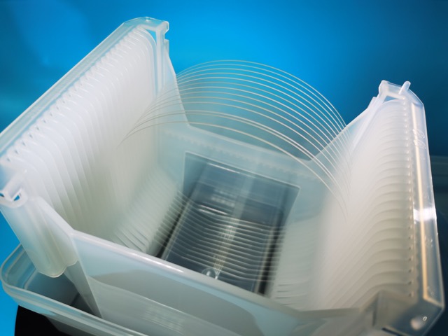


Packing and Shipping:
Sapphire Substrate Packaging and Shipping
Sapphire substrate products are securely packaged with a protective
bubble wrap, foam, and corrugated cardboard box to ensure safe and
efficient delivery. All packages are shipped via a reliable,
trackable courier service to guarantee timely and undamaged
delivery.
For international orders, all shipments must pass international
customs and may be subject to additional fees or taxes. Customers
are responsible for any applicable customs, duties, or taxes.


