300-900nm LN-On-Silicon LiNbO3 Lithium Niobate Wafer Thin Films
Layer On Silicon Substrate
Lithium niobate (LiNbO3) crystal is an important photoelectric material, and is widely used
in integrated optics, nonlinear optics, optoelectronic components,
and other fields, one of the most important substrate materials. At present, lithium niobate crystals are widely used in surface
acoustic wave, electro-optical modulation, laser Q-switching,
optical gyro, optical parametric oscillation, optical parametric
amplification, optical holographic storage, and other devices,
which play an important role in mobile phones, television, optical
communication, laser ranging, electric field detector and other
devices.
Our production of lithium niobate single crystal thin film has a
single crystal lattice structure, maintaining the physical
properties of the bulk material, with a diameter of 3 inches, the
thickness of the upper lithium niobate single crystal thin film is
0.3-0.7 microns, the middle layer is 1-micron thick silica (SiO2),
and the bottom layer is 0.5 mm thick lithium niobate wafer
substrate.
Characteristic Specification
| 300-900 nm Lithium Niobate Thin Films (LNOI) |
| Top Functional Layer |
| Diameter | 3, 4, (6) inch | Orientation | X, Z, Y etc. |
| Material | LiNbO3 | Thickness | 300-900 nm |
| Doped (optional) | MgO | | |
| Isolation Layer |
| Material | SiO2 | Thickness | 1000-4000 nm |
| Substrate |
| Material | Si, LN, Quartz, Fused Silica etc. |
| Thickness | 400-500 μm |
| Optional Electrode Layer |
| Material | Pt, Au, Cr | Thickness | 100-400 nm |
| Structure | Above or Under SiO2 Isolation Layer |
Related Customized Thin Films
| Customized Lithium Niobate & Lithium Tantalate Thin Films |
| Top Layer/ Details | Substrate Details | Top Layer Thin Films Details |
| Multi Layer Structure | Patterned Electrode & Waveguide | Different Material (SiO2/Si, Si, Sapphire, Quartz etc.) | PPLN | Special Size | Electrode (Au, Pt, Cr, Al etc.) | Orientation (Same as Bulk Wafers ) | Doped (MgO, Fe, Er, Tm etc.) |
| 100-1000 nm LiNbO3 | √ | √ | √ | √ | √ | √ | √ | √ |
| 100-1500 nm LiTaO3 | √ | √ | √ | | √ | √ | √ | √ |
5-50 um LiNbO3 | √ | | √ | | √ | | √ | |
5-50 um LiTaO3 | √ | | √ | | √ | | √ | |
Application of LN-On-Silicon
1, optical fiber communication, such as waveguide modulator, etc.
Compared with traditional products, the volume of devices produced
by using this thin film material can be reduced by more than one
million times, the integration is greatly improved, the response
bandwidth is wide, the power consumption is low, the performance is
more stable, and the manufacturing cost is reduced.
2, electronic devices, such as high quality filters, delay lines,
etc.
3, information storage, and can realize high density information
storage, a 3 inch film information storage capacity of 70 t (100000
CD)
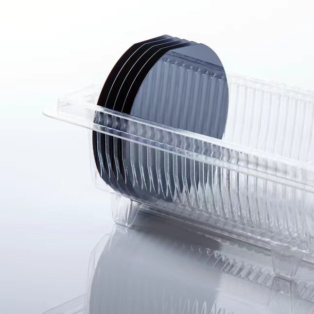
Display of Lithium Niobate Wafer Thin Films Layer On Silicon
Substrate

FAQ –
Q: What you can supply logistics and cost?
(1) We accept DHL, Fedex, TNT, UPS, EMS, SF and etc.
(2) If you have your own express number, it's great.
If not, we could assist you to deliver. Freight=USD25.0(the first
weight) + USD12.0/kg
Q: How to pay?
T/T, Paypal, West Union, MoneyGram, Secure payment and Trade
Assurance on Alibaba and etc..
Q: What's the MOQ?
(1) For inventory, the MOQ is 5pcs.
(2) For customized products, the MOQ is 5pcs-20pcs.
It depends on quantity and technics
Q: Do you have inspection report for material?
We can supply detail report for our products.
Packaging – Logistics
we are concerned with each detail of the package, cleaning,
anti-static, and shock treatment. According to the quantity and
shape of the product,
we will take a different packaging process!


