SiO2 wafer Thermal Oxide Laver Thickness 20um+5% MEMS Optical
Communication System
Product Description:
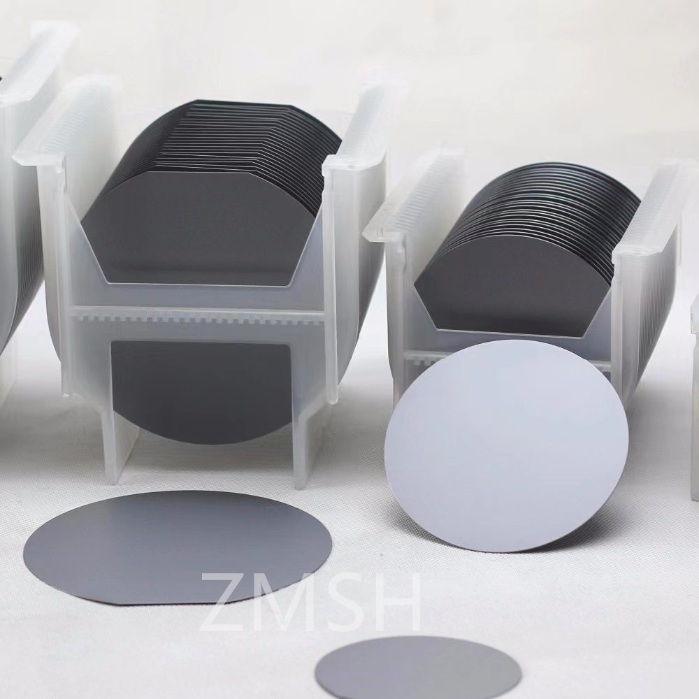
The SIO2 silicon dioxide wafer serves as a foundational element in
semiconductor manufacturing. Featuring a thickness ranging from
10μm to 25μm, this crucial substrate is available in 6-inch and
8-inch diameters, ensuring versatility for various applications.
Primarily, it acts as an essential insulating layer, playing a
pivotal role in microelectronics by providing high dielectric
strength. Its refractive index, approximately 1.4458 at 1550nm,
ensures optimal performance across diverse applications.
Renowned for its uniformity and purity, this wafer stands as an
ideal choice for optical devices, integrated circuits, and
microelectronics. Its properties facilitate precise device
fabrication processes and support technological advancements.
Beyond its foundational role in semiconductor manufacturing, it
extends its reliability and functionality to a spectrum of
applications, guaranteeing stability and efficiency.
With its exceptional attributes, the SIO2 silicon dioxide wafer
continues to drive innovations in semiconductor technology,
enabling advancements in fields such as integrated circuits,
optoelectronics, and sensor technologies. Its contributions to
cutting-edge technologies underscore its significance as a
cornerstone material in the realm of semiconductor production.

Features:
- Product Name: Semiconductor Substrate
- Refractive Index: 550nm Of 1.4458 ± 0.0001
- Boiling Point: 2,230° C (4,046° F)
- Application Areas: Semiconductor Manufacturing, Microelectronics,
Optical Devices, Etc.
- Thickness: 20um,10um-25um
- Molecular Weight: 60.09
- Semiconductor Material: Yes
- Substrate Material: Yes
- Applications: Semiconductor Manufacturing, Microelectronics,
Optical Devices, Etc.

Technical Parameters:
| Parameter | Specification |
| Thickness | 20um,10um-25um |
| Density | 2533 Kg/m-3 |
| Oxide thickness tolerance | +/- 5% (both Sides) |
| Application Areas | Semiconductor Manufacturing, Microelectronics, Optical Devices,
Etc. |
| Melting Point | 1,600° C (2,912° F) |
| Thermal Conductivity | Around 1.4 W/(m·K) @ 300K |
| Refractive Index | Approximately 1.44 |
| Molecular Weight | 60.09 |
| Coefficient of Expansion | 0.5 × 10^-6/°C |
| Refractive Index | 550nm Of 1.4458 ± 0.0001 |
| Ultra-thick silicon oxide wafer | Applications |
| Surface oxidation | Ultra-thin wafer |
| Thermal Conductivity | Around 1.4 W/(m·K) @ 300K |
Applications:
- Thin-Film Transistors: Employed in the production of TFT devices.
- Solar Cells: Used as a substrate or insulating layer in photovoltaic
technology.
- MEMS (Micro-Electro-Mechanical Systems): Crucial for MEMS device development.
- Chemical Sensors: Utilized for sensitive chemical detection.
- Biomedical Devices: Employed in various biomedical applications.
- Photovoltaics: Supports solar cell technology for energy conversion.
- Surface Passivation: Aids in semiconductor surface protection.
- Waveguides: Used in optical communication and photonics.
- Optical Fibers: Integral in optical communication systems.
- Gas Sensors: Employed for gas detection and analysis.
- Nanostructures: Used as a substrate for nanostructure development.
- Capacitors: Utilized in various electrical applications.
- DNA Sequencing: Supports applications in genetic research.
- Biosensors: Used for biological and chemical analysis.
- Microfluidics: Integral in microfluidic device fabrication.
- Light-Emitting Diodes (LEDs): Supports LED technology in various applications.
- Microprocessors: Essential for the production of microprocessor devices.
 Customization:
Semiconductor Substrate
Brand Name: ZMSH
Model Number: Ultra-thick silicon oxide wafer
Place of Origin: China
Our Semiconductor Substrate is designed with high thermal
conductivity, surface oxidation and ultra-thick silicon oxide
wafer. It has a thermal conductivity of around 1.4 W/(m·K) @ 300K
and melting point of 1,600° C (2,912° F). The boiling point is
2,230° C (4,046° F) and the orientation is
<100><11><110>. The molecular weight of this
substrate is 60.09.
Support and Services:
We provide technical support and service for our Semiconductor
Substrate product. Our team of experts is available to answer any
questions you may have about the product and its features. We can
also provide assistance in troubleshooting any issues you encounter
while using the product. We also offer remote assistance for those
who need it. Our support team is available during normal business
hours, and we can be reached by phone, email, or through our
website.
Packing and Shipping:
Packaging and Shipping for Semiconductor Substrate:
- Packaged products should be handled with care. Use a protective
covering such as bubble wrap or foam whenever possible.
- If possible, use multiple layers of protective covering.
- Label the package with the contents and destination.
- Ship the package using an appropriate shipping service. Consider
using a service with tracking capabilities.
FAQ:
- Q: What is the brand name of Semiconductor Substrate?
- A: The brand name is ZMSH.
- Q: What is the model number of Semiconductor Substrate?
- A: The model number is Ultra-thick silicon oxide wafer.
- Q: Where is Semiconductor Substrate made?
- A: It is made in China.
- Q: What is the purpose of Semiconductor Substrate?
- A: Semiconductor Substrate is used in the fabrication of integrated
circuits, microelectromechanical systems and other microstructures.
- Q: What is the feature of Semiconductor Substrate?
- A: The features of Semiconductor Substrate include low thermal
expansion coefficient, high thermal conductivity, high mechanical
strength and excellent temperature resistance.


